Wide and Parallel Wins
DWDM is the Future of Scale-Up Networking
By Nick Harris, Founder and CEO, Lightmatter
Last week, the Optical Compute Interconnect (OCI) Multi-Source Agreement (MSA) published its v1.0 line interface specification—a 24-page document co-authored by NVIDIA, Meta, Microsoft, OpenAI, Broadcom, and AMD that defines the optical physical layer for AI scale-up interconnects. It specifies Dense Wavelength-Division Multiplexing (DWDM) wavelength channels in the O-band (around 1300 nm) on a single bidirectional (BiDi) fiber, micro-ring resonators for modulation, and an external laser source architecture.
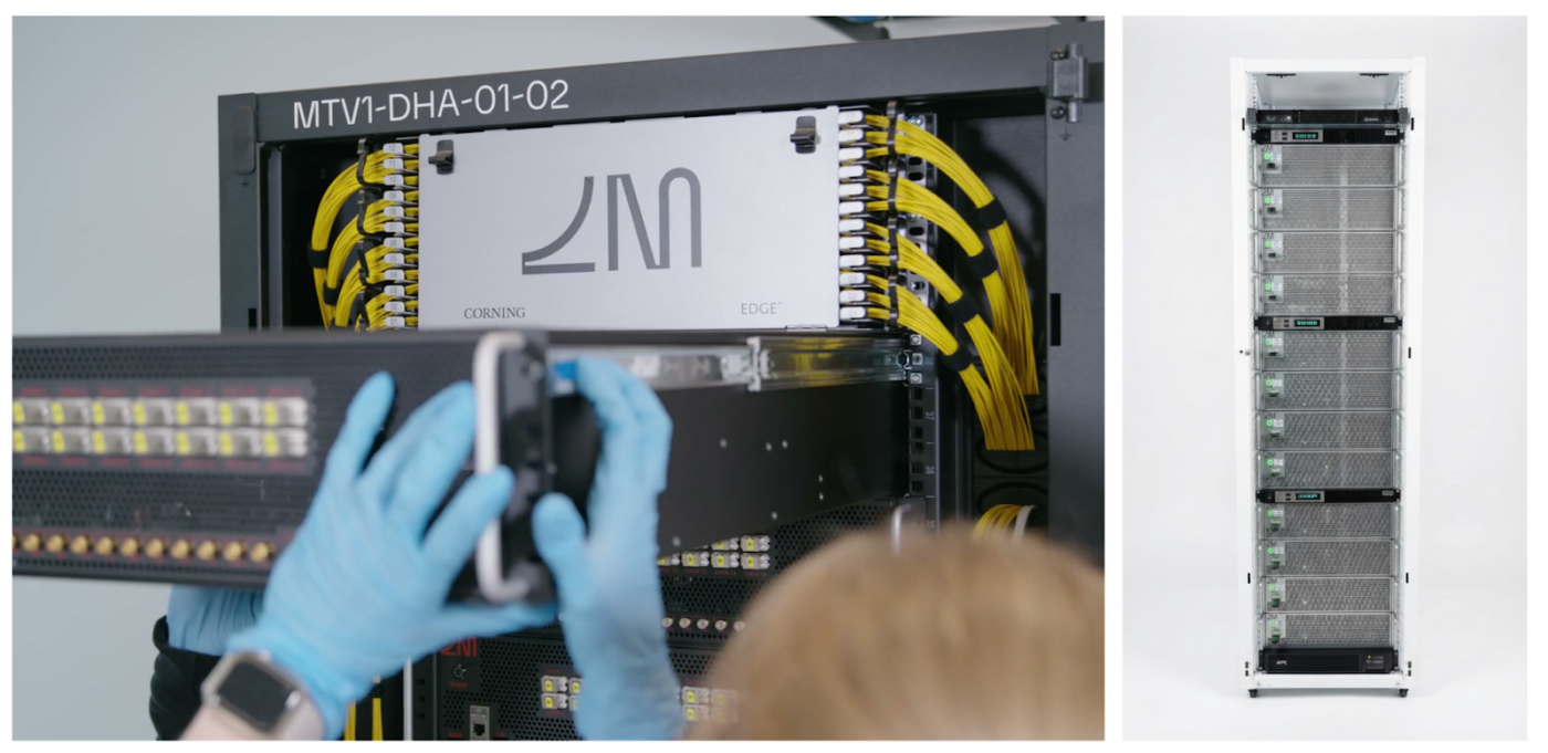
This convergence confirms that the industry is aligning on a path guided by fundamental physical constraints and first principles. At Lightmatter, we have three generations of DWDM PassageTM interconnect silicon that meet the MSA specification, racked and stacked in our validation data centers, along with our Guide® external laser source (ELS), based on our Very Large Scale Photonics (VLSPTM) technology, to power them. We’re demonstrating these record-setting platforms at OFC this week—stop by our booth!
Start from First Principles: BiDi and DWDM
In an AI scale-up fabric, radix is everything. The number of direct connections each accelerator can make to its peers determines collective bandwidth, all-reduce performance, and ultimately how fast your model trains. More connections, better cluster. You want as many as you can possibly run.
The problem is the fiber plant—the cables, connectors, and routing hardware that ties the whole cluster together. Every fiber is a cost, a failure mode, and a hard physical constraint. At some point, the physical density of the fiber plant becomes the binding constraint—not compute, not memory, not the silicon. The interconnect fabric inside an AI cluster is already one of the most fiber-dense environments humans have ever built, and it gets dramatically worse as clusters scale from tens of thousands of accelerators to hundreds of thousands.
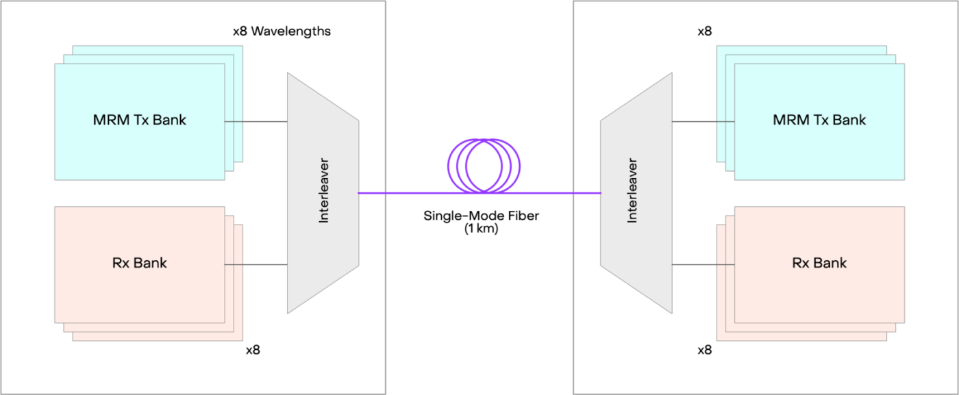
The first unlock is bidirectional fiber. A conventional optical link uses one fiber for transmit (TX) and one for receive (RX)—so every logical connection consumes two fibers. Run TX and RX in the same fiber using separate wavelength bands, and you’ve immediately doubled the number of logical connections your fiber plant can support. Same cables, same connectors, same routing. Twice the radix.
The second unlock is DWDM. Once you’re running BiDi, the question becomes how much bandwidth you can carry on each of those links. For short-reach, high-density cluster links, the answer isn’t higher-order modulation. PAM4 and PAM8 pack more bits per symbol, but the tighter eye opening drives up your pre-Forward Error Correction (FEC) Bit Error Rate (BER) floor—which means you need stronger FEC (with higher power consumption) to close the link, which adds pipeline latency in the SerDes. In AI scale-up, where collective operation performance is latency-sensitive, and customers are actively minimizing FEC overhead, that’s a real tax. The bill for PAM4 gets worse as you scale the cluster and the latency budget tightens. You’re paying in power, silicon area, and latency. NRZ per DWDM channel sidesteps all of it: the link budget at these distances is forgiving, the receivers are simple, and you can run minimal FEC.
The OCI spec defines exactly this architecture. Group A wavelengths (1308–1315 nm) travel in one direction; Group B (1328–1335 nm) travels the other way on the same fiber. Four DWDM channels per group, each at 53.125 Gbaud NRZ, aggregate to 212.5 Gbps per direction per fiber. BiDi doubles your radix. DWDM maximizes the bandwidth of every link. Together, they’re the right answer from first principles.
Three generations of Lightmatter’s Passage hardware in silicon today support up to 16-wavelength DWDM bidirectional links from 53.125 Gbaud NRZ to 53.125 Gbaud PAM4 (106.25 Gbps).
We already have hundreds of Passage platforms spanning three generations operating on this exact architecture in our validation data center. In 2025, Lightmatter demonstrated 800 Gbps on a single fiber with a 16-wavelength, 53.125 Gbaud NRZ, bidirectional link—the world’s first at that milestone. In another step forward, we also sampled a breakthrough 1,600 Gbps-per-fiber, 16-wavelength, 53.125 Gbaud PAM4 Passage platform that we built in collaboration with Qualcomm.
Micro-Rings and the External Laser Source
The OCI spec also specifies the modulation technology: cascaded micro-ring modulators (MRMs) driven by an external laser source (ELS). This is worth unpacking because it reflects a fundamental design philosophy that we’ve long believed is correct for co-packaged optics at scale.
MRMs are extraordinarily compact and power-efficient. A ring resonator is a wavelength-selective filter—it couples light from a bus waveguide into a ring when the ring circumference is resonant with the optical wavelength. By applying a bias to a heater or junction to tune the ring, you switch it on and off resonance, which modulates the light. The device footprint is tiny, the drive voltage is low, and you can pack them densely on a silicon photonic chip.
The barrier to entry for MRMs is high. Reaping their power efficiency and area density advantages demands serious engineering effort in stabilization, sequencing, and monitoring. MRMs must be made resilient to rapid thermal transients—800°C/sec and beyond—and require intricate sequencing for multi-wavelength operation, in which unique rings must be assigned to specific wavelengths. Even with all of that working, there’s another layer: firmware validation at scale. Firmware that works on a handful of systems reveals entirely new failure modes at hundreds of systems. At Lightmatter, we’ve built deep expertise in MRM control and sequencing over 8 years and multiple generations of silicon. For new entrants, building a chip with MRMs is the first step on a multi-year journey—one with spectacular upside over every other modulation technology.
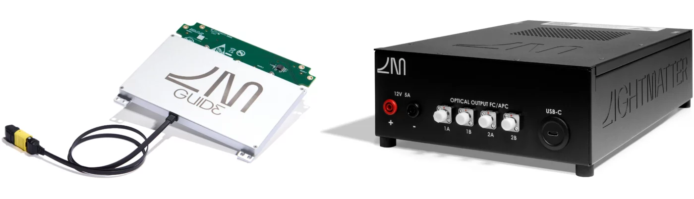
Guide 1 is sampling today, features unprecedented wavelength accuracy and stability, and already supports 16 wavelengths at 200- and 400-GHz spacing.
The catch is that lasers and hot silicon don’t mix. A co-packaged optical engine sits directly on or next to a GPU or switch — one of the hottest components in the data center. Laser reliability drops dramatically with temperature, and laser output power also decreases, reducing wall-plug efficiency. And when a laser does fail — and they do — you need to be able to replace it without pulling the whole compute package. The external laser source solves all of this by physically separating the laser from the heat source. The ELS operates off-chiplet, feeding continuous-wave light into the optical engine via a single-mode fiber. The rings do the modulation. The ELS spec requires narrow linewidth (≤1 MHz), high SMSR (≥30 dB), and tight wavelength accuracy across all eight channels — because the laser’s job is to be a stable, replaceable, thermally isolated light source, nothing more.
Guide is Lightmatter’s ELS based on VLSP technology — a single photonic chip integrating hundreds of lasers, purpose-built for co-packaged optical systems. The industry has long relied on assembling individual laser diodes on submounts with epoxy and wire bonds, including lenses and isolators — discrete, fragile, and expensive to manufacture at scale. Guide 1 changes that: hundreds of lasers on a single chip, no glue joints, far fewer failure points.
Why This Moment Matters
Lightmatter’s portfolio spans the full link architecture roadmap—from 112G and 224G PAM4 links shipping today to the massively parallel DWDM architectures that scale-up fabrics are moving toward.
Industry specifications matter because they coordinate investment across a supply chain. When NVIDIA, Meta, OpenAI, Microsoft, Broadcom, and AMD agree on a common optical physical layer, that signals to every ODM, every fiber vendor, every connector manufacturer, and every optical engine startup that there is a real market to build toward. The OCI MSA spec is that signal.
For Lightmatter, this MSA represents alignment with a strategy we’ve been driving since the company’s founding. The Guide and Passage product lines were designed around the assumption that DWDM, co-packaged optics, and external laser sources would become the standard architecture for AI scale-up. We reasoned from physics, built the hardware, demonstrated the records, and engaged the ecosystem.
Learn more about Lightmatter’s Guide laser platform and Passage interconnect at lightmatter.co. The OCI MSA specification is available at oci-msa.org.