PHOTONIC CHIPS FOR AI
Lightmatter's 8X Leap: World-First 16-Wavelength Bidirectional Optical Link for AI Data Centers
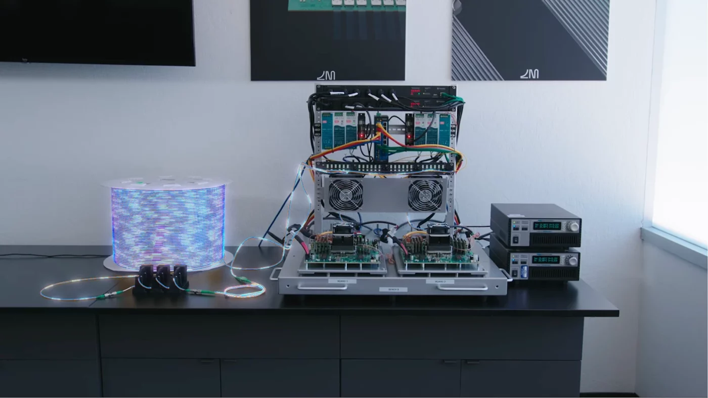
World-first 16-wavelength bidirectional optical DWDM Link on a strand of standard single mode fiber. This Lightmatter breakthrough represents an 8X leap in bidirectional fiber bandwidth density and a doubling of radix, paving the way for the next generation of AI data centers.
Passage M1000: Powering the Next 1000x in AI Performance
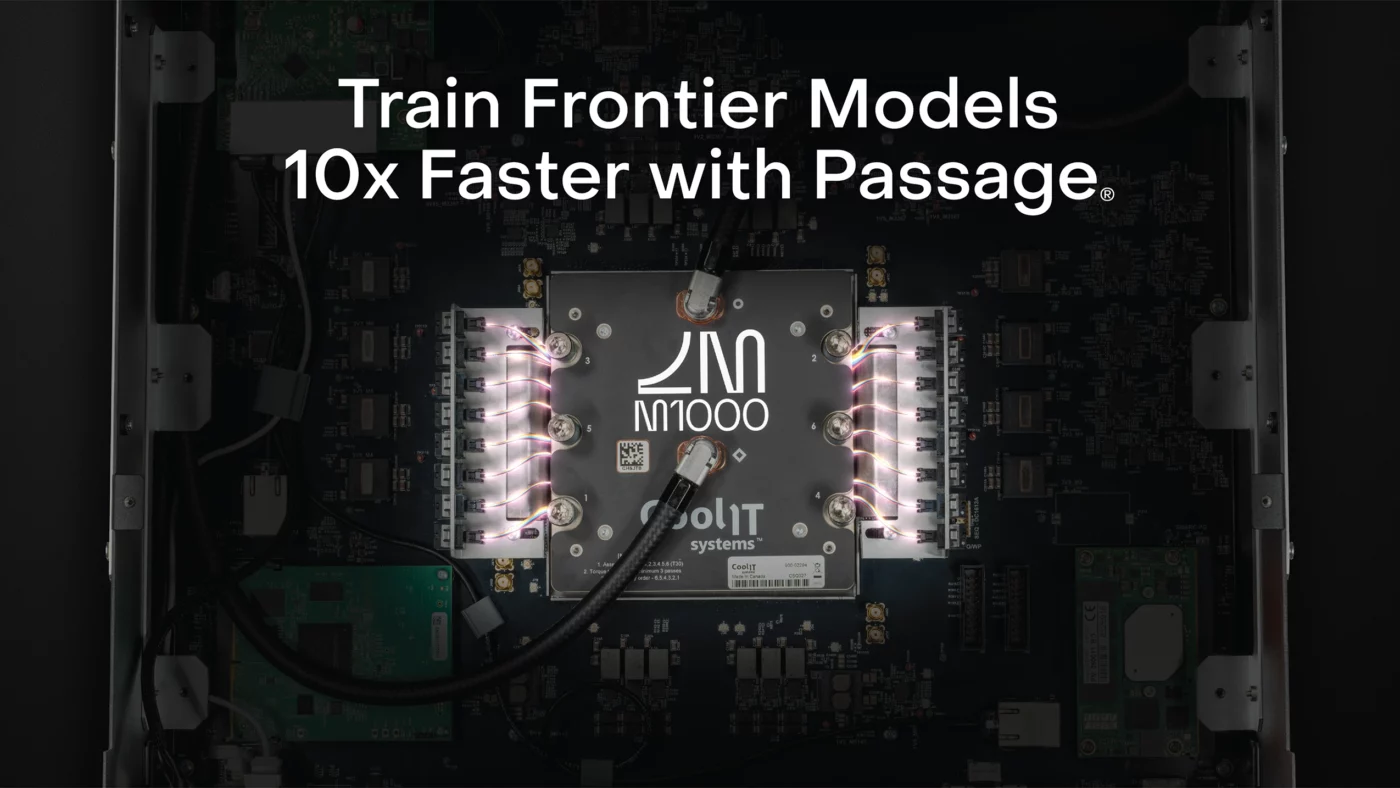
Explore the Passage M1000 Reference System, a groundbreaking platform built around the Passage M1000 3D Photonic Superchip. Discover how this revolutionary photonic interconnect technology is changing the game for Artificial Intelligence (AI) infrastructure by enabling massive scale-up bandwidth and radix,
3D Co-Packaged Optics (CPO) that Redefine AI Interconnect with Edgeless I/O Technology
Lightmatter is leading CPO innovation by delivering the world’s fastest photonic interconnects for next-generation AI infrastructure.
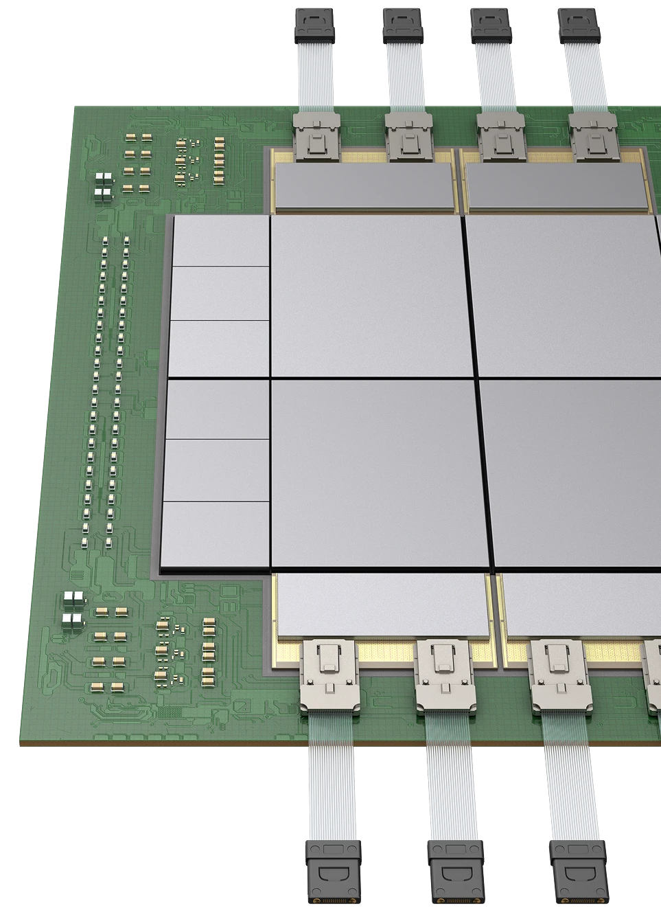
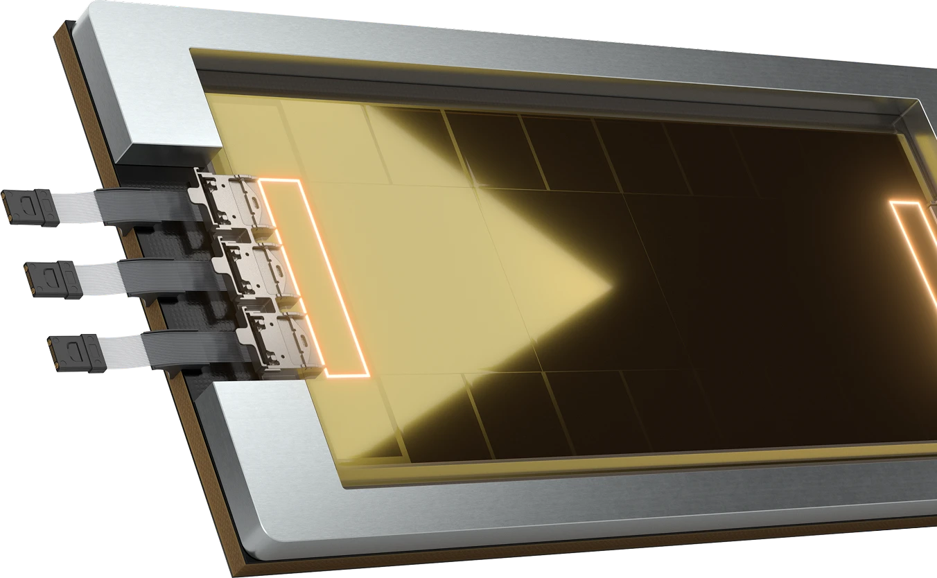
Our groundbreaking 3D Co-Packaged Optics technology features an industry-first Edgeless I/O architecture, fundamentally transforming data movement. By vertically stacking an Electronic Integrated Circuit (EIC) directly with a Photonic Integrated Circuit (PIC) within a single, highly dense I/O chiplet, we eliminate conventional shoreline limitations.
This revolutionary design creates a compact, high-bandwidth optical engine that provides unparalleled bandwidth density and power efficiency necessary to scale AI infrastructure for decades to come.
From 3D Photonics Breakthrough
to
High-Volume Deployment
Lightmatter’s CPO technology is the foundation for next-generation AI infrastructure. Our photonic interconnect platform is massively scalable, enabling us to address the spectrum of AI interconnect solutions, with lane speeds from 56G NRZ to 448G PAM4, bidirectional or unidirectional, and up to 16 wavelengths. Passage optical engines also support standard and advanced packaging flows.
Bi-Directional WDM Example
Each color represents a different wavelength, carrying a separate, high-bandwidth optical data stream.
Passage L-Series Linear Drive CPO
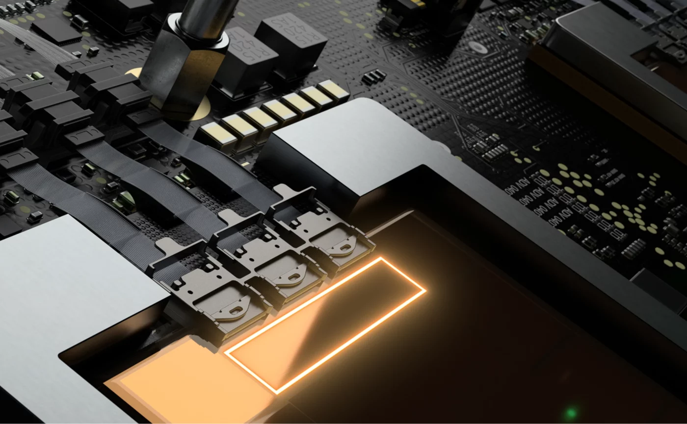
The imminent shift to optical interconnects demands uncompromising performance within current standards. Passage L-Series Co-Packaged Optics is a direct application of our scalable photonics architecture, engineered to deliver industry-leading bandwidth density and energy efficiency in standard packages and link formats.
The L-Series Linear Drive solution simplifies the path to high-performance CPO, providing a standards-compliant, high-volume optical engine that ensures your AI compute is always connected with optimal bandwidth and power.
Near-Packaged Optics (NPO)
Not every deployment requires a chip-package modification. Our Near-Packaged Optics (NPO) delivers the flexibility and performance of Lightmatter’s advanced interconnect technology in a modular, highly accessible format.
By deploying an L-Series module directly on the PCB, you instantly gain the high bandwidth and long reach of optics without modifying your existing package.
This “everything on board” approach is the ideal, low-risk, high-volume path for early adoption of cutting-edge Passage photonics, accelerating your time-to-market with proven Passage performance.
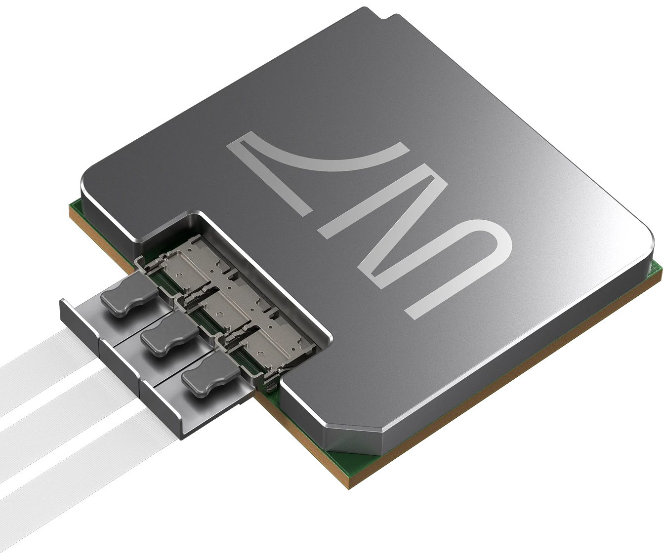
Detachable Fiber Technology
Mass deployment of high-performance Co-Packaged Optics requires simplified assembly and maintenance. Lightmatter’s Detachable Fiber Attach Technology sets a new standard for interconnect deployability and field serviceability.
High-Volume Scalability (HVM)
Our approach enables wafer-level, V-groove-less passive alignment, ensuring placement accuracy is independent of pitch scaling. This results in a significantly higher assembly yield by allowing known good optical units to be validated before final package assembly.
Serviceability and Reliability
This detachable format makes fiber maintenance and replacement simple and low-risk in the data center environment, ensuring maximum uptime for mission-critical AI workloads.
Rack-Scale Validation System
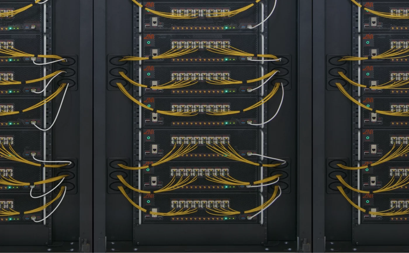
Lightmatter operates in its facilities a state-of-the-art rack-scale validation platform that incorporates our photonic interconnects. This allows us to rigorously test and validate the quality, reliability, and performance of our products at the scale and density demanded by next-generation AI datacenters. We’re delivering proven readiness, de-risking the deployment of cutting-edge optical interconnects for hyperscalers, bridging the gap between CPO innovation and mass deployment.
Driving photonics standardization
Lightmatter is working across leading industry standards organizations to push the envelope of AI interconnect and networking standards and propel AI infrastructure into the photonic era.


Accelerating AI Through Ecosystem Collaboration
Lightmatter is at the forefront of silicon photonics innovation, fostering collaboration in leading industry associations like the Global Semiconductor Alliance (GSA), the Open Compute Project (OCP) Foundation and Optica, promoting open standards to drive adoption of advanced optical interconnect technologies that unlock the full potential of AI.
Additional Resources
Passage L-Series
For more information about the Passage™ L-Series co-packaged optics (CPO) platform, scaling next gen XPUs and switch applications.
Passage M-Series
Learn about the Passage™ M-Series, an advanced reference platform capable of delivering more than 100 Tbps total bandwidth per package.
Silicon Photonics Knowledge Hub
Explore the foundational principles of photonic integrated circuits (PICs) and photonic interconnects, including co-packaged optics (CPO).
