Passage
3D Photonic Interconnect Platform
Passage® pushes the frontier of photonic link design and packaging technologies—delivering chips with record-breaking energy efficiency, bandwidth, and reliability. Edgeless I/O architecture enables unlimited bandwidth scaling.
Form Factors
Complete Photonics Roadmap
Passage is available in both L- and M-series form factors, covering the entire spectrum from pluggable optics to 3D integration.
The Edgeless I/O Advantage
Traditional chip I/O—electrical and optical—is confined to die edges (shoreline). As die area scales (r²), perimeter only scales linearly (2πr), creating a bandwidth bottleneck.
Passage Solution: 3D vertical integration allows I/O placement across the entire die area. Bandwidth density scales with area (mm²), providing unlimited scaling headroom.
Near Package

L-Series NPO
10x pluggable bandwidth at a fraction of the energy. Minimized latency with linear-drive architecture.
On Board

L-Series OBO
10x pluggable bandwidth in an ultra-high-density serviceable module. Retimer required for extreme reach.
Co-Packaged

L-Series CPO
High-efficiency, high-bandwidth chips co-packaged directly with XPU and switches.
Interposer Co-Packaged

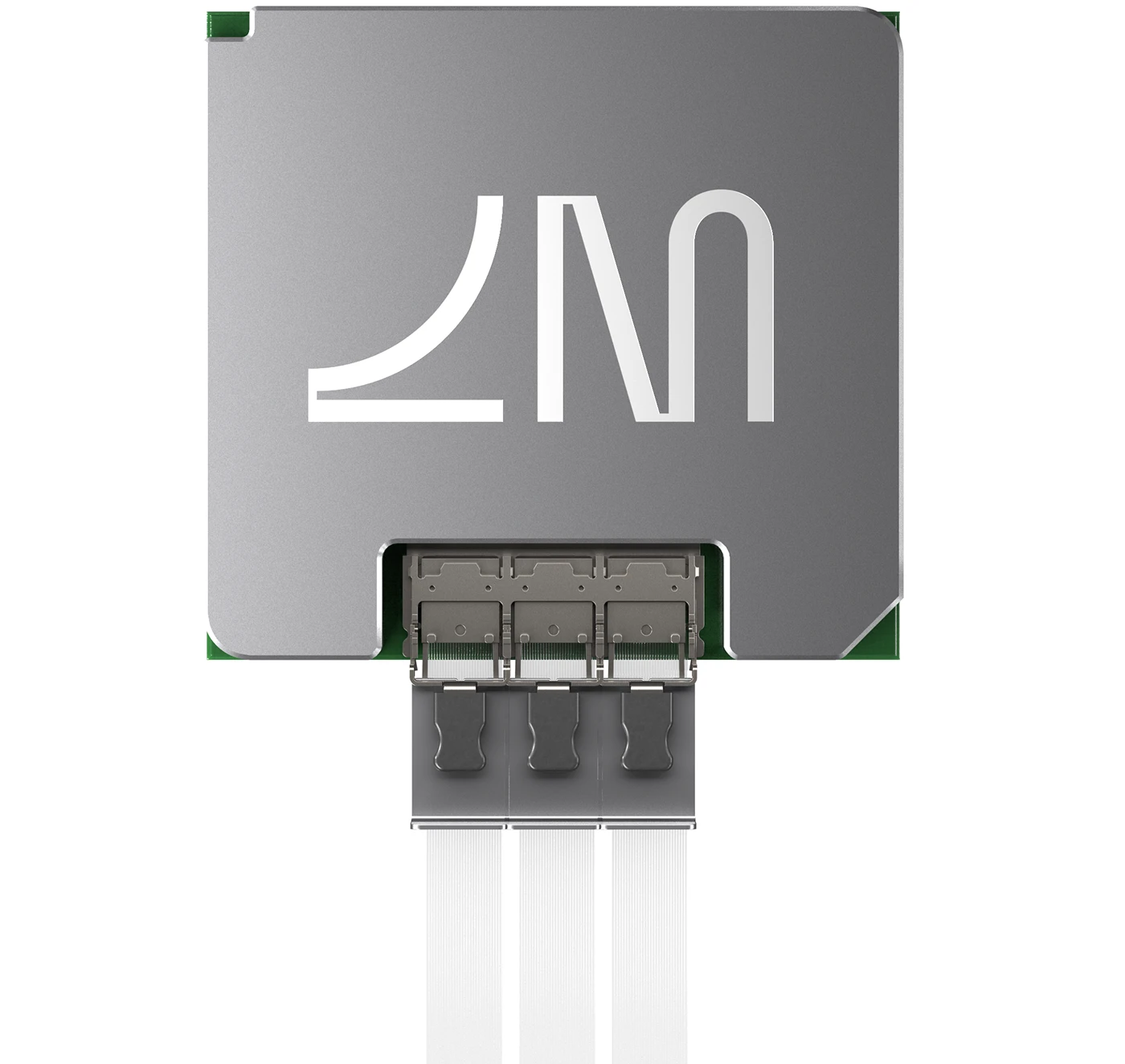
M-Series
The ultimate in energy efficiency, bandwidth density, and speed. Edgeless I/O architecture.
Reliability at Scale
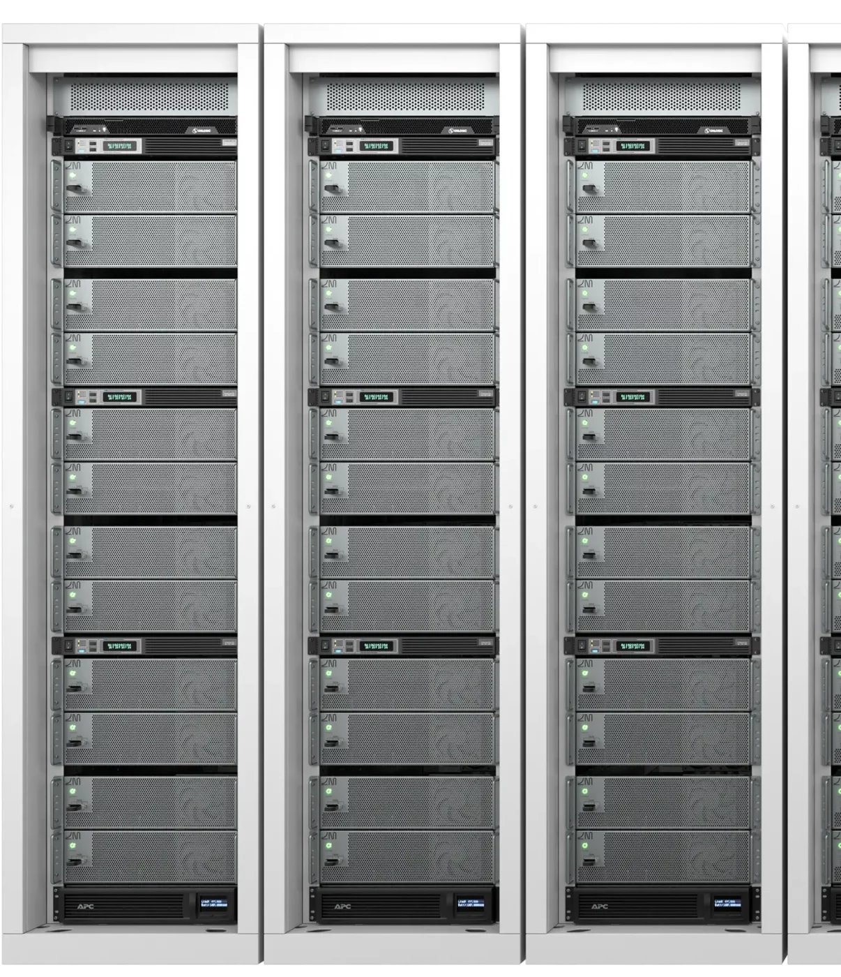
Rack-Scale Validation System
Lightmatter operates in its facilities state-of-the-art rack-scale validation platforms that incorporate our photonic interconnects. This allows us to rigorously test and validate the quality, reliability, and performance of our products at the scale and density demanded by next-generation AI datacenters.
We’re delivering proven readiness, de-risking the deployment of cutting-edge optical interconnects for hyperscalers, bridging the gap between CPO innovation and mass deployment.