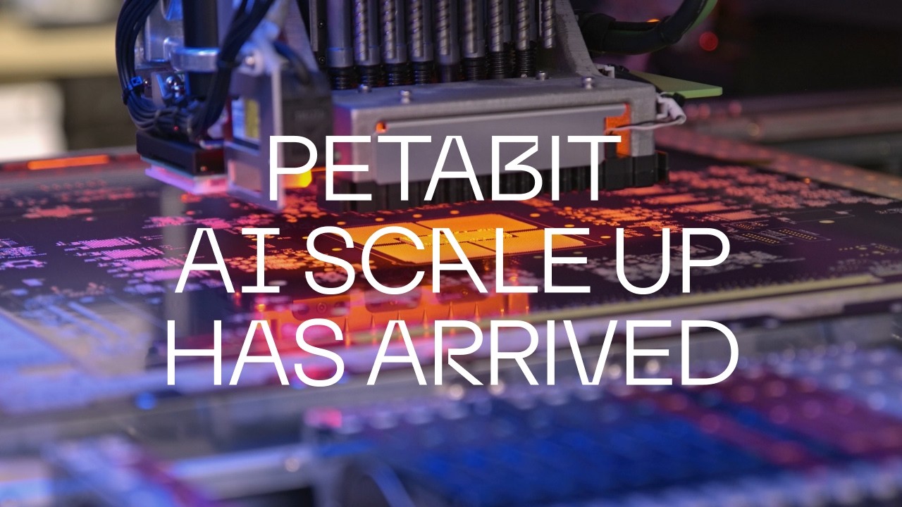
Lightmatter Silicon Photonics, from Wafer to Rack: How the World’s Fastest AI Interconnects are Made
Ever wonder how a cutting-edge silicon photonics chip goes from a wafer to a fully assembled data center rack? In this video, Lightmatter takes you inside the end-to-end manufacturing journey using the example of our Passage M1000 3D photonic interposer — from wafer fabrication at leading foundries to integration and testing at the largest outsourced semiconductor assembly and test companies to final board-level assembly.
What you’ll see:
• How Silicon-on-insulator (SOI) wafers become silicon photonic chips — through lithography, deposition, etching, and CMP — each with thousands of optical links
• Wafer-level photonic testing and measurements to validate optical engines and detachable coupler loss
• Flip-chip bonding,dicing, and advanced packaging of optical engines
• Detachable Fiber Array Unit (FAU) assembly — eClick and vClick
• Board-level integration and final rack assembly of Lightmatter Passage® photonic chips for AI
Lightmatter’s Passage platform delivers up to 114 Tbps of optical bandwidth, redefining AI data center interconnect with co-packaged optics (CPO) and our Guide Light Engine.