Scale-Up is a Problem Made for Photonics
NVIDIA’s announcement at GTC Taipei 2026 that NVLink Fusion will extend to photonic interconnects marks a pivotal moment where AI infrastructure scaling meets the inevitable demands of physics. Lightmatter is bringing Passage interconnects and Guide lasers to NVLink Fusion.
A scale-up fabric carries collectives across every accelerator in the domain, and the slowest link sets the step time. Collective operations like all-reduce, all-gather, and all-to-all stress different traffic patterns, but the workload mix demands high bandwidth and bounded latency between accelerators. Decode is the tightest case: every generated token requires all accelerators to synchronize their data under a service-level objective, and any lag directly throttles the token rate. Per-accelerator bandwidth requirements scale with domain size, and the largest domains are the ones that require NVLink Fusion photonics.
Scale-up requires enormous bandwidth in a small footprint. The binding constraint is electrical bandwidth density feeding the photonics. Photonics is not the limiter: a single fiber carries terabits with dense wavelength division multiplexing (DWDM), and photonic chip surface density runs well beyond that. The bottleneck is how much electrical bandwidth you can deliver to the photonic interface. Today, long-reach electrical SerDes, the interface that carries scale-up traffic between packages, deliver 1-2 Tbps per millimeter of shoreline. The industry-standard die-to-die UCIe interface over advanced packaging reaches a density of 8-20 Tbps per millimeter, but remains confined inside the package. Both are linear regimes, bounded by the die perimeter. Passage breaks that bound by moving the electrical-to-optical interface off the shoreline. The M-series places it across the full die area, delivering on the order of 1 Tbps/mm² of areal I/O density. The L-series brings the same shift in near-package, on-board, and co-packaged optical engine form factors. Each form factor opens scale-up domains that electrical interconnect alone cannot reach.
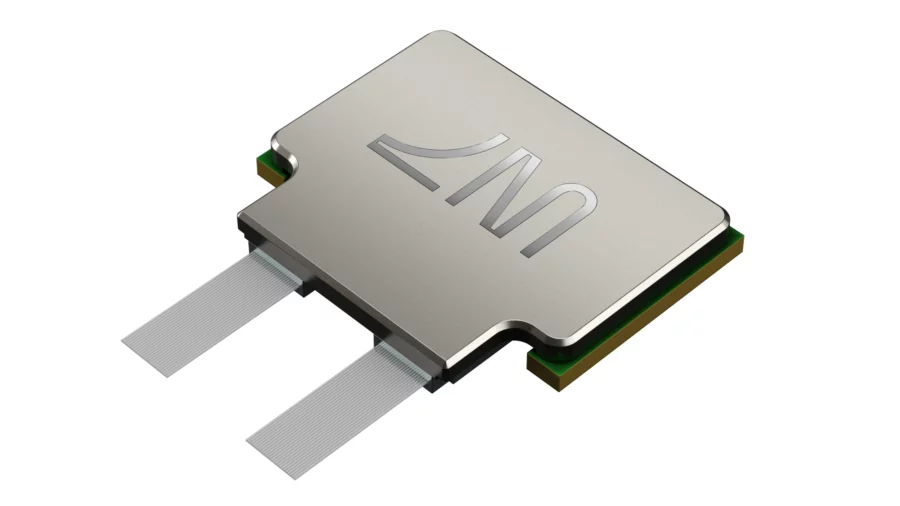
Passage L20 Photonic Interconnect PlatformWith Passage, the bandwidth carried on an optical fiber is set by the wavelengths multiplexed onto it, not by the perimeter of the chip that drives it. Bandwidth is decoupled from the chip shoreline limitations for the first time. Reach extends from a meter to a kilometer without requiring any architectural change for the host XPU. This is only made possible by a photonic interconnect in the package fed by an external laser source–what Lightmatter has been building for eight years.
Passage is our photonic interconnect platform. The L-series delivers near-package, on-board, and co-packaged photonics. The M-series is a 3D photonic interposer that places I/O across the entire die area rather than along the package shoreline. Three generations of Lightmatter silicon operate in our validation data center, spanning bidirectional 800 Gbps per fiber on Passage EVK50, 1.6 Tbps per fiber on Passage EVK100, and 114 Tbps of aggregate bidirectional bandwidth on the M1000 reference platform at 2.3 pJ/bit, including laser power. Passage covers every form factor a customer integrating optical NVLink Fusion will consider.
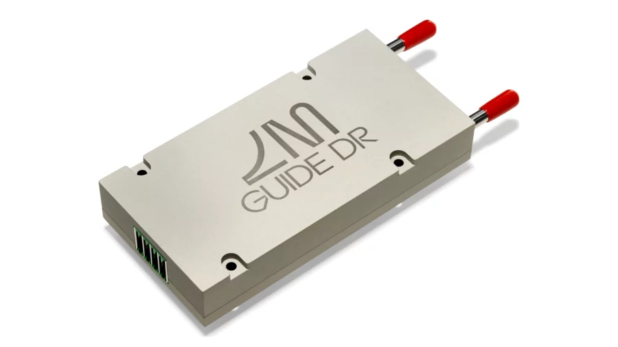
Guide is our external laser source, built on Very Large Scale Photonics, our integration approach for consolidating hundreds of laser diodes onto a single photonic chip. A single Guide 1 module enables 51.2 Tbps of I/O on a 16-wavelength DWDM grid centered at 1310 nm, replacing nine conventional ELSFP laser modules with one chip. It also offers unprecedented wavelength stability and accuracy–critical for next-generation DWDM optical engines–and self-healing capabilities.
Both products are aligned to the OCI MSA, the optical physical layer co-authored by NVIDIA and other industry leaders: bidirectional fibers, DWDM in the O-band, micro-ring modulation, and external laser sources. Lightmatter is the first to have silicon validated against that specification today.
NVLink Fusion with Passage will enable scale-up domains in the thousands of XPUs, accelerating the most important AI workloads to levels only possible with photonic interconnects. We are committed to building this with NVIDIA and with the customers who will operate at this scale.
The next generation of AI factories will be built on light.
Nick Harris, Ph.D. Founder and CEO