Passage M1000 EVK
3D Photonic Interposer for Exascale AI
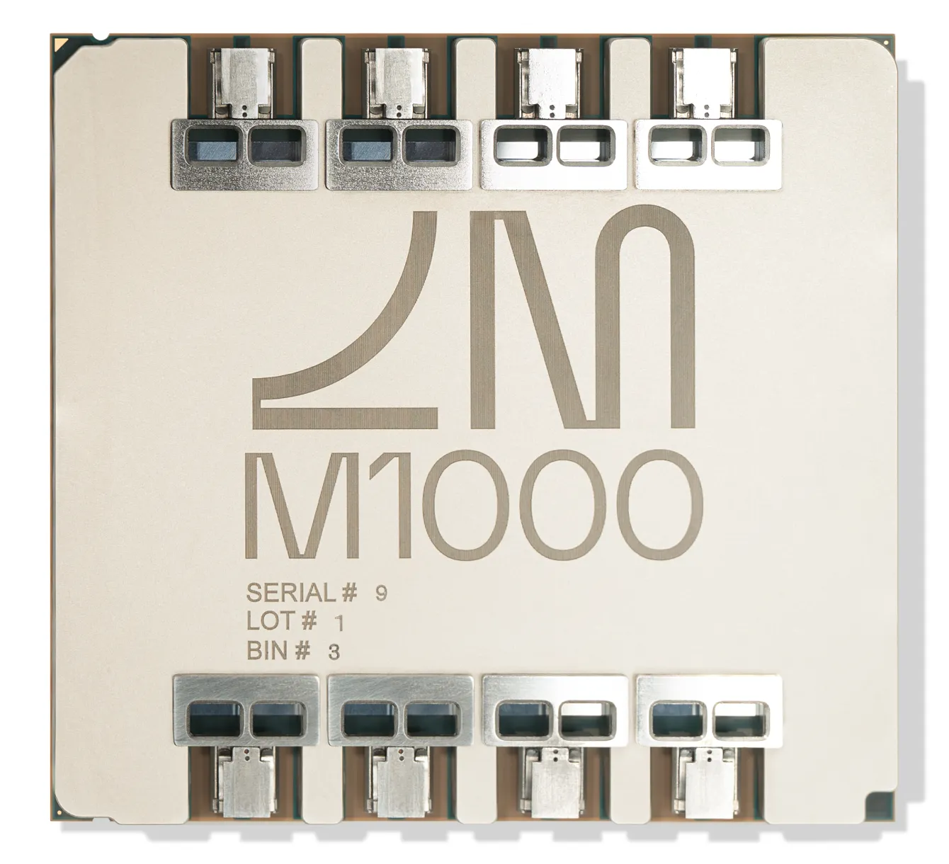
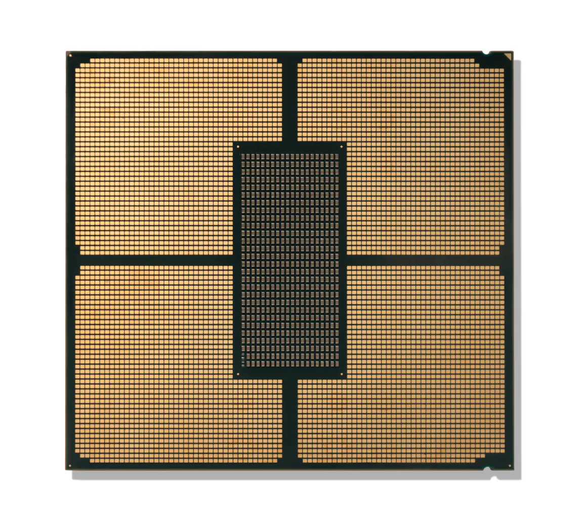
The M1000 is the world’s first 3D Photonic Superchip. The M1000 reference platform consists of a server with all components needed to operate the chip. An array of 32 I/O chiplets and two thermal load chips are 3D stacked in a chip-on-wafer process on the M1000 photonic interposer. M1000 eliminates the “shoreline bottleneck” by allowing any chip on its surface to direct all of its I/O bandwidth to the optical fibers, enabling unbound bandwidth for next-generation AI accelerators and switches. Detachable fiber array units at a massive scale enable serviceability for a record-breaking platform.
Data rate
114.6
Tbps Total Bi-Directional
System Efficiency
2.3
pJ/bit incl. laser power; SerDes ~2.0 pJ/bit
Fiber Attach
Detachable
Field-Serviceable
Challenge
The Shoreline Bottleneck
Traditional chips are limited by their perimeter (shoreline), which is where I/O devices for communication reside. As chips get larger, the edge-to-area ratio drops, starving the core of bandwidth.
This fundamental geometric limit sets a bound on how much I/O bandwidth can escape a chip and therefore limits AI scaling.
Perimeter-Limited Chip
I/O confined to the edge. Core bandwidth starved.
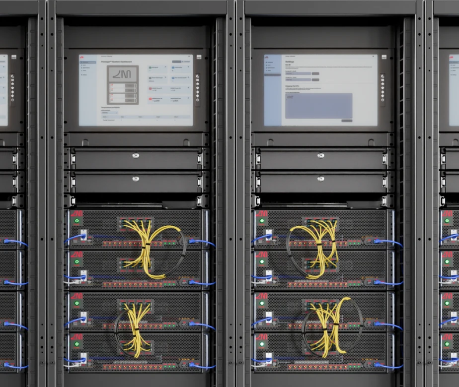
Innovation
Edgeless I/O Architecture
M1000 is the world’s first photonic interposer—a 3D stack of advanced-node ASICs with hundreds of SerDes integrated on the Passage PIC. All of these ASICs escape their full bandwidth, even if they don’t have access to the package shoreline Chip-on-wafer packaging. Edgeless I/O.
01 – Architecture
Edgeless I/O
We don’t just use the edge. We use the entire 4,000 mm² surface for connectivity. Eliminate energy-draining network-on-chip journeys by placing I/O directly where it’s needed.
02 - Advanced Packaging
Unprecedented Density
Chip on wafer on substrate architecture to integrate multiple high-performance dies onto a single interposer, a production-ready solution for complex AI and HPC applications.
03 — Power
Powered by Guide
The Guide VLSP light engine supports the M1000 with 8-wavelength DWDM. Unprecedented optical power and reliability for massive scale.
04 — Topology
Optical Circuit Switching
Integrated optical routing layer allows dynamic configuration of network topologies both inside the package and outside using solid-state photonics. Key capability enhancing the resiliency and deployment flexibility of the infrastructure.
1 Million XPUs
and Beyond
Passage M1000 technology enables unprecedented scale-up and scale-out connectivity, linking millions of accelerators across the datacenter with photonic bandwidth.
M1000 Platform
Engineered for Rack Scale
The M1000 evaluation kit demonstrates 3D photonic integration at scale, from chip-level innovation to rack-scale deployment.
Edgeless I/O Interposer
A 4,000 mm² photonic interposer with 256 fiber connections for high-density optical integration.
Detachable Fibers with eClick Optics
Enabling serviceability and repair in the field.
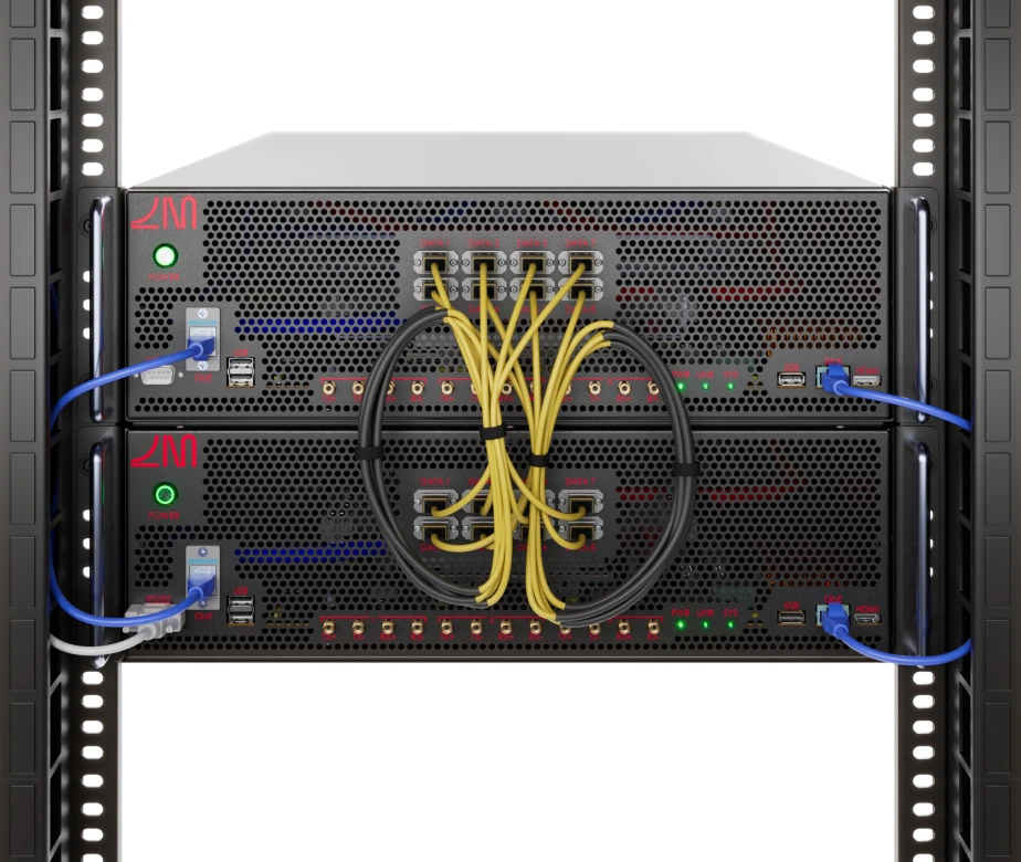
Rack-Scale Validation
Passage M1000 EVK is deployed in our validation data center.
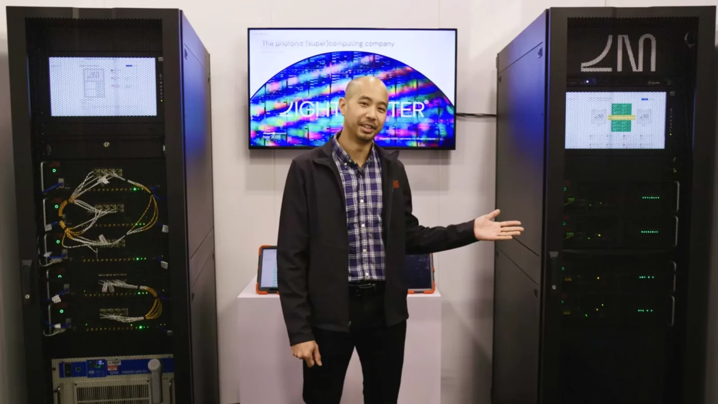
Comprehensive SDK
The M1000 EVK is supported by a comprehensive SDK designed for deep performance characterization and validation.
Link Quality Analysis
Real-time Bit Error Rate (BER) monitoring at 56 Gbps NRZ for comprehensive link validation.
Advanced Telemetry
Sensing for power delivery, thermal gradients, and optical path health.
Liquid-Cooling Ready
Integrated into a liquid-cooled 19” 3U server environment to manage high-density thermal loads.
Technical Specifications
Get Started with M1000 EVK
Connect with our sales team to discuss M1000 integration for your AI infrastructure roadmap.