Seeing is Believing: A Technical Deep Dive into Lightmatter’s Hardware
It’s been a busy summer at Lightmatter.
For the last four months, we have been demonstrating our production-ready Passage™ 3D photonic interconnect hardware to the world’s largest hyperscalers and semiconductor companies. At the recent Hot Interconnects (HOTI) and Hot Chips (HOTC) conferences, we lifted the curtain on the systems and performance data our partners have witnessed live in our labs.
Hot Interconnects: Redefining Performance and Efficiency
At HOTI, we showcased the world’s first 16-wavelength (16λ) bidirectional link running on one single-mode optical fiber. Our dozens of complete, rackable platforms showcase a generational leap in co-packaged optics (CPO) performance, significantly surpassing current industry benchmarks.
The results speak for themselves:
- Massive Bandwidth: Our Passage link operates with 16 bidirectional wavelengths to deliver 800 Gbps on a single fiber.
- Unprecedented Efficiency: The system achieves wall-plug efficiency of 4.6 pJ/bit, inclusive of the 2.6 pJ/bit for the photonics and external light source (Guide), and ~2 pJ/bit for an off-the-shelf XSR SerDes co-packaged with Passage.
- Robust Performance: With over 1 kilometer of standard fiber and six connectors, we achieve an open-eye, FEC-less Bit Error Rate (BER) of less than 10-9 (typically 10-12).
This is enabled by Lightmatter’s proprietary Microring Modulator (MRM) control algorithms, a foundational element of a performance-optimized system architecture. Compared to legacy Mach-Zehnder Modulators (MZMs) or Electro-Absorption Modulators (EAMs), MRMs offer a staggering reduction in size and power. An MZM can be up to 5,000 µm long and consume 50 mW, while our MRMs are just 5-15 µm in diameter and consume as little as 1 mW, which is also 10x smaller and 10x more energy-efficient than EAMs.
Conventional MRMs have long suffered from thermal stability challenges. Lightmatter MRMs have solved this. In Figure 1, we present the results of testing a Passage link with a rapid temperature aggressor, using a swept tunable laser to achieve an effective 50 nm/s ramp rate over a 4 nm range—representing an 800℃/s temperature aggressor. The system maintains a robust link BER of less than 10-9 (pre-FEC) while undergoing this extreme thermal aggression scenario.
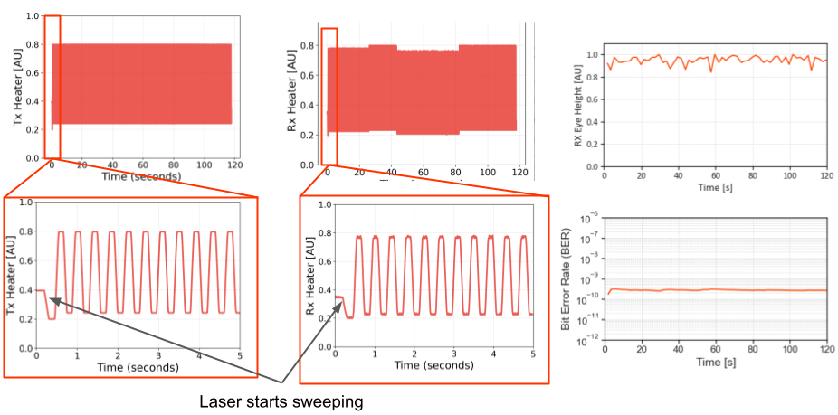
Figure 1: Rapid Temperature Cycling and BER Performance
As seen in Figure 2 and the linked video, our production-ready control technology maintains a stable connection even when the hardware is repeatedly thermally cycled from 25°C to 105°C. These slower-ramp temperature cycling tests have been run for over 30 hours, with the system consistently achieving a raw BER below 10-9.

Figure 2: Extended Thermal Cycling and BER Performance. Here, testing of a worst-case 1-kilometer Passage link with 16 MRMs with Lightmatter control and stabilization results in all lanes reporting raw (pre-FEC) BERs better than 10-9, well below the forward error-correction threshold.
Hot Chips: A Tour of the Passage M1000 Platform
At HOTC, Lightmatter’s founder and chief scientist, Darius Bunandar, presented our Passage M1000 3D photonic interposer and server platform. Capable of supporting large multi-chip packages, the M1000 is a “superchip” photonic platform built to eliminate the interconnect bottleneck. M1000 is an entire interconnect substrate that sits directly beneath partner chips (e.g., XPUs and switches). The 4,000 mm2 silicon die complex features 34 integrated chiplets, 1024 SerDes lanes, and 256 optical fibers to deliver up to 114 Tbps of total bandwidth. This density is only possible because of Lightmatter’s advanced photonic engine design. By pairing our MRMs with an inductorless driver, we’ve created an incredibly compact transmitter and receiver pair, occupying approximately the area of a microbump (10x smaller than EAMs and 100,000x smaller than MZIs).
The M1000 platform delivers state-of-the-art performance, with wide-open eye diagrams, achieving a TDECQ of less than 1 dB, well below the maximum 3.4 dB specified in IEEE 802.3. Furthermore, the M1000 platform is designed for resilience. It features Lightmatter’s reconfigurable Optical Circuit Switching (OCS), which allows data to be dynamically rerouted to backup optical paths in the event of a fiber or component failure. We’ve also proven the platform’s ability to handle the immense thermal load from co-packaged chips, demonstrating stable operation with power densities exceeding 1.4 W/mm2 (supporting multi-kilowatt XPU complexes), as shown in Figure 1.
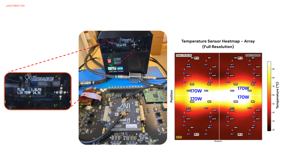
Figure 3: Power Delivery and Thermal Load Testing. Our lab testing, which incorporates a 369 mm2 thermal test chip, has validated Passage M1000’s power density of 1.47W/mm2, while delivering >2.5A/mm2 through its TSVs.
Production-Ready Hardware
Lightmatter’s presentations at HOTI and HOTC detailed (some of) what we have built and demonstrated to dozens of the world’s largest hyperscalers and semiconductor companies over the summer. Passage is built on a world-class, production-ready manufacturing ecosystem with industry leaders like Amkor, ASE, GlobalFoundries, Tower, and TSMC.
This marks a turning point for silicon photonics, making scalable hardware available as the industry is poised to adopt photonics for the inevitable transition to CPO interconnects in AI data centers. We’re thrilled to be providing our partners with the stable, proven technology needed to solve their biggest challenges and build the next generation of AI.
The future of AI interconnect is here.
Nick Harris, Ph.D.
Founder and CEO