Passage

A Wafer-Scale, Programmable Photonic Interconnect

Enabling arrays of heterogeneous chips to communicate with unprecedented bandwidth and energy efficiency.

Passage Interconnect

Transistors and photonics integrated side-by-side provide a simple, yet powerful interface that facilitates dynamic reconfiguration of the communications topology. This integration allows 40 passage lanes to fit in the space of a single optical fiber, reducing packaging complexity and cost while dramatically increasing performance.

Performance

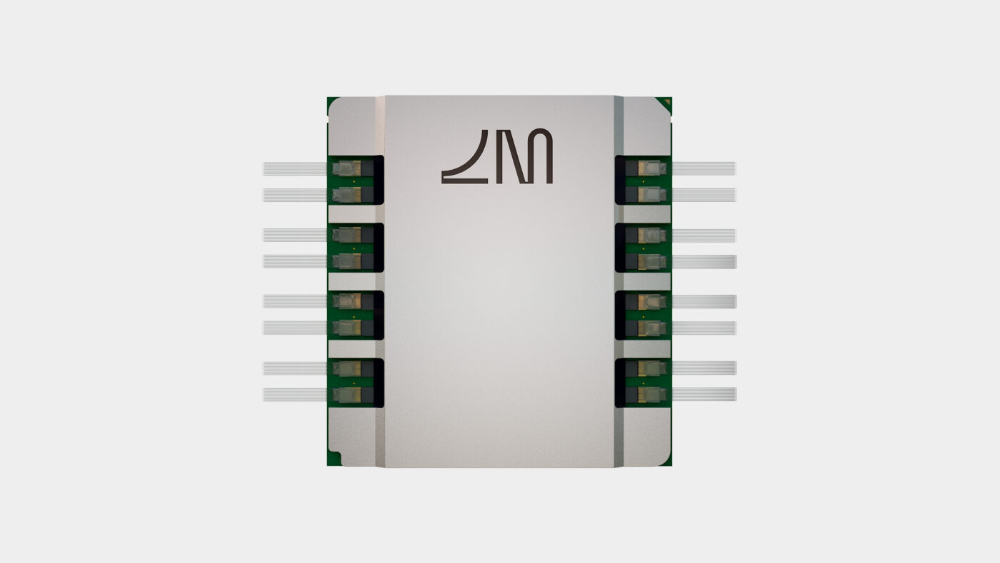
Dramatic interconnect density improvement. 40 waveguides in the space of one optical fiber.

Input/output bandwidth from each chiplet site for full reticle. And up to 250+ Tbps per chiplet site edge.

More bandwidth than existing chip-to-chip interconnect solutions.

Chiplet to chiplet latency, single hop connectivity between every site.

Features

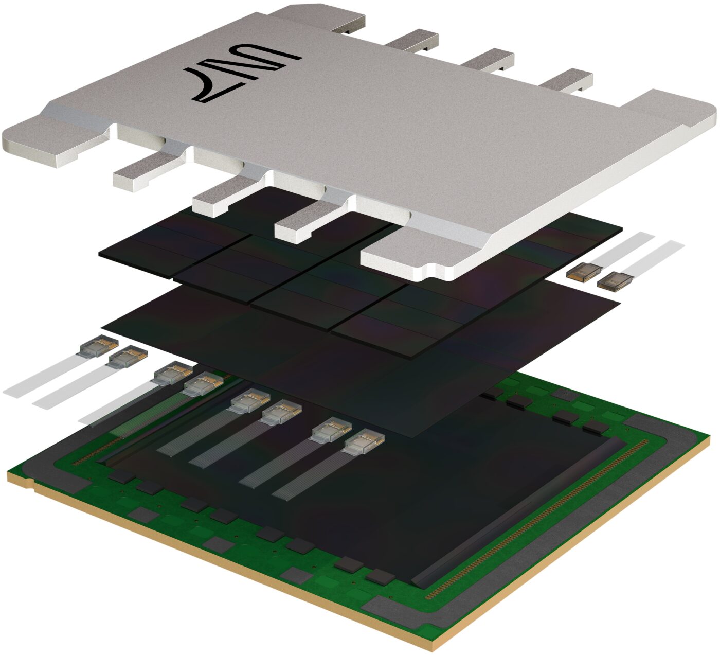
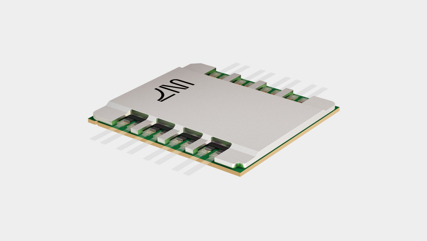
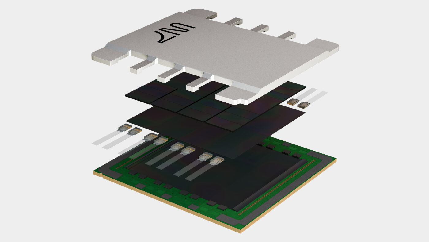
Fully integrated chiplet, interconnect solution with direct fiber attach all in a single assembly.

Uniform architecture for flexible dicing (e.g. 2×2, 2×4, 2×8).

Wafer-scale processing with heterogeneous tiles of CPUs, GPUs, FPGAs, DRAM, and ASICs.

Transistors and photonics integrated side-by-side. SerDes signals from chiplets directly modulated onto waveguides. Standards-based D2D interfaces supported including UCIe, AIB, and others.

Any Topology Anytime with 1-Hop-Everywhere. Dynamically reconfigure network configurations in microseconds.

Thousands of waveguides with cross-reticle stitching. Every chiplet directly connected to every other at multi-terabit speed and near-zero latency.

Economics

Functionality of a rack on a single chip.

Completely eliminates rats-nests of external fibers required by alternative CPO solutions.

Fiber-to-chip attach is expensive. Optical interconnect between chips is built into the platform. No fiber-attach required.

Completely integrated photonic fabric – no fiber attaches required. Highly-optimized form-factor supporting multitude of configurations in far less space.

  • Accelerates any application that requires high bandwidth inter-chip communication, including AI model training, large-scale ML inference, HPC, and core routing
  • Dynamic topology reconfiguration capability with algorithms that automatically compute the shortest distance between two communicating sites
  • Communication error detection using cyclic redundancy checks
  • Dynamic choice of communication protocols between PAM-2, PAM-4, or PAM-8

  • Attaching optical fibers to chips is extremely expensive. Passage has built-in photonic interconnect and no fibers to attach, which means reduced complexity. By removing the need for driving long wire traces between computer chips and optical transceivers, Passage achieves 5x more energy efficient communications with 200x more bandwidth—reducing operating costs for high performance computing systems
  • Build your wafer scale solution with Passage: advanced 5nm / 7nm ASICs has low fabrication yield. Building a wafer-scale ASIC chip has a very low probability of yield success. With Passage, we can cherry pick those chips that have yielded and place them on Passage to create a wafer-scale high-performing computer system with photonic interconnect
  • Reconfiguring a network used to require an engineer plugging out and in hundreds of optical fiber connections between chips. Passage enables topology reconfigurations within a mere millisecond

Interested in partnering with us?